- 您现在的位置:买卖IC网 > Sheet目录324 > FAN3217TMX (Fairchild Semiconductor)IC GATE DRIVER DUAL 2A 8-SOIC
�� �
�
�Layout� and� Connection� Guidelines�
�The� FAN3216� and� FAN3217� gate� drivers� incorporate�
�fast-reacting� input� circuits,� short� propagation� delays,�
�and� powerful� output� stages� capable� of� delivering� current�
�peaks� over� 2� A� to� facilitate� voltage� transition� times� from�
�under� 10� ns� to� over� 150� ns.� The� following� layout� and�
�connection� guidelines� are� strongly� recommended:�
�?�
�Keep� high-current� output� and� power� ground� paths�
�separate� from� logic� input� signals� and� signal� ground�
�paths.� This� is� especially� critical� for� TTL-level� logic�
�thresholds� at� driver� input� pins.�
�?�
�?�
�?�
�?�
�?�
�Keep� the� driver� as� close� to� the� load� as� possible� to�
�minimize� the� length� of� high-current� traces.� This�
�reduces� the� series� inductance� to� improve� high-�
�speed� switching,� while� reducing� the� loop� area� that�
�can� radiate� EMI� to� the� driver� inputs� and�
�surrounding� circuitry.�
�If� the� inputs� to� a� channel� are� not� externally�
�connected,� the� internal� 100� k� Ω� resistors� indicated�
�on� block� diagrams� command� a� low� output.� In� noisy�
�environments,� it� may� be� necessary� to� tie� inputs� of�
�an� unused� channel� to� VDD� or� GND� using� short�
�traces� to� prevent� noise� from� causing� spurious�
�output� switching.�
�Many� high-speed� power� circuits� can� be� susceptible�
�to� noise� injected� from� their� own� output� or� other�
�external� sources,� possibly� causing� output� re-�
�triggering.� These� effects� can� be� obvious� if� the�
�circuit� is� tested� in� breadboard� or� non-optimal� circuit�
�layouts� with� long� input� or� output� leads.� For� best�
�results,� make� connections� to� all� pins� as� short� and�
�direct� as� possible.�
�FAN3216� and� FAN3217� are� pin-compatible� with�
�many� other� industry-standard� drivers.�
�The� turn-on� and� turn-off� current� paths� should� be�
�minimized,� as� discussed� in� the� following� section.�
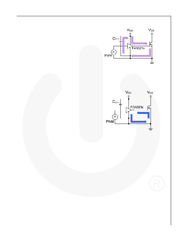
�Figure� 32.� Current� Path� for� MOSFET� Turn-On�
�Figure� 33� shows� the� current� path� when� the� gate� driver�
�turns� the� MOSFET� OFF.� Ideally,� the� driver� shunts� the�
�current� directly� to� the� source� of� the� MOSFET� in� a� small�
�circuit� loop.� For� fast� turn-off� times,� the� resistance� and�
�inductance� in� this� path� should� be� minimized.�
�Figure� 33.� Current� Path� for� MOSFET� Turn-Off�
�Figure� 32� shows� the� pulsed� gate� drive� current� path�
�when� the� gate� driver� is� supplying� gate� charge� to� turn� the�
�MOSFET� on.� The� current� is� supplied� from� the� local�
�bypass� capacitor,� C� BYP� ,� and� flows� through� the� driver� to�
�the� MOSFET� gate� and� to� ground.� To� reach� the� high�
�peak� currents� possible,� the� resistance� and� inductance� in�
�the� path� should� be� minimized.� The� localized� C� BYP� acts�
�to� contain� the� high� peak� current� pulses� within� this� driver-�
�MOSFET� circuit,� preventing� them� from� disturbing� the�
�sensitive� analog� circuitry� in� the� PWM� controller.�
�?� 2009� Fairchild� Semiconductor� Corporation�
�FAN3216� /� FAN3217� ?� Rev.� 1.0.3�
�13�
�www.fairchildsemi.com�
�发布紧急采购,3分钟左右您将得到回复。
相关PDF资料
FAN3223CMX
IC GATE DVR DUAL INV 4A 8-SOIC
FAN3226CMPX
IC GATE DVR DUAL 2A 8-MLP
FAN3227TMPX
IC GATE DVR DUAL 2A 8-MLP
FAN3268TMX
IC BRIDGE DVR P/N-CH 2A 8SOIC
FAN3278TMX
IC BRIDGE DVR P-N 2A 30V 8-SOIC
FAN5331SX
IC LED DRVR WHITE BCKLGT SOT23-5
FAN5333ASX
IC LED DRVR WHITE BCKLGT SOT23-5
FAN5340MPX
IC LED DVR SYNC CC 8-MLP
相关代理商/技术参数
FAN3217TMX_12
制造商:FAIRCHILD 制造商全称:Fairchild Semiconductor 功能描述:Dual-2A, High-Speed, Low-Side Gate Drivers
FAN3217TMX_F085
功能描述:功率驱动器IC Intgrtd Load Switch RoHS:否 制造商:Micrel 产品:MOSFET Gate Drivers 类型:Low Cost High or Low Side MOSFET Driver 上升时间: 下降时间: 电源电压-最大:30 V 电源电压-最小:2.75 V 电源电流: 最大功率耗散: 最大工作温度:+ 85 C 安装风格:SMD/SMT 封装 / 箱体:SOIC-8 封装:Tube
FAN3223
制造商:FAIRCHILD 制造商全称:Fairchild Semiconductor 功能描述:Dual 4A High-Speed, Low-Side Gate Drivers
FAN3223_10
制造商:FAIRCHILD 制造商全称:Fairchild Semiconductor 功能描述:Dual 4A High-Speed, Low-Side Gate Drivers
FAN3223_11
制造商:FAIRCHILD 制造商全称:Fairchild Semiconductor 功能描述:Dual 4A High-Speed, Low-Side Gate Drivers
FAN3223_12
制造商:FAIRCHILD 制造商全称:Fairchild Semiconductor 功能描述:Dual 4A High-Speed, Low-Side Gate Drivers
FAN3223C
制造商:FAIRCHILD 制造商全称:Fairchild Semiconductor 功能描述:30V PMOS-NMOS Bridge Driver
FAN3223CMPX
功能描述:功率驱动器IC Dual 4A High-Speed Low-Side Gate RoHS:否 制造商:Micrel 产品:MOSFET Gate Drivers 类型:Low Cost High or Low Side MOSFET Driver 上升时间: 下降时间: 电源电压-最大:30 V 电源电压-最小:2.75 V 电源电流: 最大功率耗散: 最大工作温度:+ 85 C 安装风格:SMD/SMT 封装 / 箱体:SOIC-8 封装:Tube